- 您现在的位置:买卖IC网 > Sheet目录985 > ISLA224IR72EV1Z (Intersil)BOARD EVALUATION FOR ISLA224P
�� �
�
�ISLA224P�
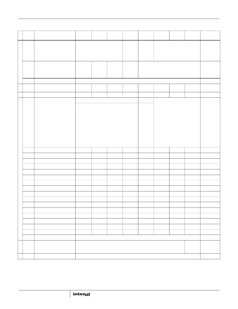
�SPI� Memory� Map� (Continued)�
�ADDR.�
�DEF.� VALUE�
�(Hex)�
�PARAMETER� NAME�
�BIT� 7� (MSB)�
�BIT� 6�
�BIT� 5�
�BIT� 4�
�BIT� 3�
�BIT� 2�
�BIT� 1�
�BIT� 0� (LSB)�
�(HEX)�
�73�
�output_mode_A�
�Output� Mode� [7:5]�
�000� =� LVDS� 3mA� (Default)�
�001� =� LVDS� 2mA�
�Output� Format� [2:0]�
�000� =� Two’s� Complement� (Default)�
�010� =� Gray� Code�
�00h�
�NOT� reset� by�
�Soft� Reset�
�100� =� LVCMOS�
�Other� codes� =� Reserved�
�100� =� Offset� Binary�
�Other� codes� =� Reserved�
�74�
�output_mode_B�
�Reserved� DLL� Range� Reserved�
�DDR�
�Reserved�
�00h�
�0� =� Fast�
�1� =� Slow�
�Default=’0’�
�Enable�
�(must� be�
�set� to� 1)�
�NOT� reset� by�
�Soft� Reset�
�75-B5�
�Reserved�
�Reserved�
�B6�
�cal_status�
�Calibration�
�Read� Only�
�Done�
�B7-BF�
�Reserved�
�C0�
�test_io�
�Output� Test� Mode� [7:4]�
�User� Test� Mode� [2:0]�
�00h�
�0� =� Off� (Note� 17)�
�1� =� Midscale� Short�
�2� =� +FS� Short�
�3� =� -FS� Short�
�4� =� Checkerboard� (Note18)�
�5-6� =� Reserved�
�7� =� All� on/� off� (Note19)�
�8� =� User� Pattern� (1� to� 8� deep)�
�9� =� Reserved�
�10� =� Ramp�
�11-15� =� Reserved�
�0� =� user� pattern� 1-2�
�1� =� cycle� pattern� 1� through� 4�
�2� =� cycle� pattern� 1� through� 6�
�3� =� cycle� pattern� 1� through� 8�
�4-7� =� NA�
�C1�
�C2�
�C3�
�C4�
�C5�
�C6�
�C7�
�C8�
�C9�
�CA�
�CB�
�CC�
�CD�
�CE�
�CF�
�D0�
�user_patt1_lsb�
�user_patt1_msb�
�user_patt2_lsb�
�user_patt2_msb�
�user_patt3_lsb�
�user_patt3_msb�
�user_patt4_lsb�
�user_patt4_msb�
�user_patt5_lsb�
�user_patt5_msb�
�user_patt6_lsb�
�user_patt6_msb�
�user_patt7_lsb�
�user_patt7_msb�
�user_patt8_lsb�
�user_patt8_msb�
�B7�
�B15�
�B7�
�B15�
�B7�
�B15�
�B7�
�B15�
�B7�
�B15�
�B7�
�B15�
�B7�
�B15�
�B7�
�B15�
�B6�
�B14�
�B6�
�B14�
�B6�
�B14�
�B6�
�B14�
�B6�
�B14�
�B6�
�B14�
�B6�
�B14�
�B6�
�B14�
�B5�
�B13�
�B5�
�B13�
�B5�
�B13�
�B5�
�B13�
�B5�
�B13�
�B5�
�B13�
�B5�
�B13�
�B5�
�B13�
�B4�
�B12�
�B4�
�B12�
�B4�
�B12�
�B4�
�B12�
�B4�
�B12�
�B4�
�B12�
�B4�
�B12�
�B4�
�B12�
�B3�
�B11�
�B3�
�B11�
�B3�
�B11�
�B3�
�B11�
�B3�
�B11�
�B3�
�B11�
�B3�
�B11�
�B3�
�B11�
�B2�
�B10�
�B2�
�B10�
�B2�
�B10�
�B2�
�B10�
�B2�
�B10�
�B2�
�B10�
�B2�
�B10�
�B2�
�B10�
�B1�
�B9�
�B1�
�B9�
�B1�
�B9�
�B1�
�B9�
�B1�
�B9�
�B1�
�B9�
�B1�
�B9�
�B1�
�B9�
�B0�
�B8�
�B0�
�B8�
�B0�
�B8�
�B0�
�B8�
�B0�
�B8�
�B0�
�B8�
�B0�
�B8�
�B0�
�B8�
�0x00�
�00h�
�00h�
�00h�
�00h�
�00h�
�00h�
�00h�
�00h�
�00h�
�00h�
�00h�
�00h�
�00h�
�00h�
�00h�
�D1-FD�
�Reserved�
�Reserved�
�FE�
�Offset/Gain_Adjust_Enable�
�Reserved�
�Enable�
�00h�
�“1”� =�
�Enable�
�FF�
�Reserved�
�Reserved�
�NOTES:�
�17.� During� Calibration� xCCCC� (MSB� justified)� is� presented� at� the� output� data� bus,� toggling� on� the� LSB� (and� higher)� data� bits� occurs� at� completion� of�
�calibration.� This� behavior� can� be� used� as� an� option� to� determine� calibration� state.�
�18.� Use� test_io� =� 0x41� for� Checkerboard� outputs� on� DDR� Outputs.�
�19.� Use� test_io� =� 0x71� for� all� ones/zeroes� outputs� on� DDR� Outputs.�
�30�
�FN7570.1�
�November� 30,� 2012�
�发布紧急采购,3分钟左右您将得到回复。
相关PDF资料
ISPTPKIT
SCREW KIT TAMPER RESISTANT 9PCS
ITCSN-0400-25-U
HEATSHRINK ITCSN 2/5" X 25'
JC2AF-TM-DC24V-F
RELAY GEN PURPOSE DPST 10A 24V
JJM1A-12V
RELAY AUTOMOTIVE SPST 20A 12V
JM1AN-ZTM-DC5V-F
RELAY GEN PURPOSE SPST 20A 5V
JQ1P-18V-F
RELAY GEN PURPOSE SPDT 10A 18V
JS1-F-6V-F
RELAY GEN PURPOSE SPDT 10A 6V
JSM1-9V-5
RELAY AUTOMOTIVE SPDT 15A 9V
相关代理商/技术参数
ISLA224P
制造商:INTERSIL 制造商全称:Intersil Corporation 功能描述:Dual 14-Bit, 250MSPS/200MSPS/130MSPS ADC
ISLA224P12
制造商:INTERSIL 制造商全称:Intersil Corporation 功能描述:High Performance Dual 14-Bit, 125MSPS ADC
ISLA224P12IRZ
制造商:Intersil Corporation 功能描述:DUAL 14-BIT 125MSPS UNBUFFERED INPUT, 72-PIN - Trays 制造商:Intersil Corporation 功能描述:IC ADC 14BIT SPI/SRL 125M 48QFN 制造商:Intersil 功能描述:Dual 14-Bit 125MSPS Unbuffered Input, 72
ISLA224P13
制造商:INTERSIL 制造商全称:Intersil Corporation 功能描述:Dual 14-Bit, 250MSPS/200MSPS/130MSPS ADC
ISLA224P13IRZ
制造商:Intersil Corporation 功能描述:DUAL 14-BIT 130MSPS UNBUFFERED INPUT, 72-PIN - Trays 制造商:Intersil Corporation 功能描述:IC ADC 14BIT SRL/SPI 72QFN 制造商:Intersil 功能描述:DL 14-BIT 130MSPS UNBUFRED INPUT 72PIN
ISLA224P20
制造商:INTERSIL 制造商全称:Intersil Corporation 功能描述:Dual 14-Bit, 250MSPS/200MSPS/130MSPS ADC
ISLA224P20IRZ
制造商:Intersil Corporation 功能描述:DUAL 14-BIT 200MSPS UNBUFFERED INPUT, 72-PIN - Trays 制造商:Intersil Corporation 功能描述:IC ADC 14BIT SRL/SPI 72QFN 制造商:Intersil 功能描述:DL 14-BIT 200MSPS UNBUFRED INPUT 72PIN 制造商:Intersil Corporation 功能描述:IC, ADC, 14BIT; Resolution (Bits):14bit; Sampling Rate:200MSPS; Supply Voltage Type:Single; Supply Voltage Min:1.7V; Supply Voltage Max:1.9V; Supply Current:375mA; Digital IC Case Style:QFN; No. of Pins:72; Data Interface:SPI ;RoHS Compliant: Yes
ISLA224P25
制造商:INTERSIL 制造商全称:Intersil Corporation 功能描述:Dual 14-Bit, 250MSPS/200MSPS/130MSPS ADC